AES-VHDL
VHDL Implementation of AES Algorithm
There are simple VHDL implementations of AES-128 encryption and decryption algorithms in this repository. This is actually my first experience in the VHDL implementation!
- AES-VHDL
- What is AES?
- Pipelined VS Loop Unrolled
- Encryption
- Decryption
- References
What is AES?
There might be a few people who deal with computers and hardwares, but have not heard the name of AES yet which is a famous symmetric block cipher. If you are among those who are not familiar with the AES, [1] is a good reference to understand how this algorithm works. This implementation is also based on [1].
Pipelined VS Loop Unrolled
Two famous kinds of hardware implementation techniques, are pipelining and loop-unrolling techniques. In pipelining, registers are inserted between each combinational processing element so that each input data block can be processed simultaneously in each processing element. An overview of a pipelined implementation of AES encryption algorithm is depicted in the following shape, where the round-i depicts the i’th round of AES encryption algorithm.

The number of rounds of AES-128 encryption is 10 and an architecture implementing this cipher is called fully pipelined, when all data blocks of 10 rounds can be processed simultaneously. For a fully pipelined implementation of AES-128 ten 128-bit data registers are needed. The more data block we want to process simultaneously, the more registers and therefore, the more area we need for implementation.
In contrast to pipelining, in a loop-unrolling technique one or multiple rounds of the algorithm are processed in the same clock cycle. In the smallest case of a loop-unrolled implementation of AES which is depicted in the following shape, only one round of the algorithm is implemented as a combinational processing element and a data register is also used to store the result obtained in the previous clock cycle.

Therefore the next plaintext must be entered after 10 clock cycles, while in a fully pipelined architecture, in each clock cycle one new plaintext can be entered to the process of encryption. Although pipelined architecture has more throughput than the loop-unrolled architecture, it uses more area than the loop-unrolled one. Therefore fully pipelined architecture offer the highest performance and is suitable for the cases in which the area is not constrained. In contrast to fully pipelined architecture, the smallest case of loop-unrolled, which is sometimes called the round based implementation, uses the lowest area and is suitable for area constrained applications. This implementation is a loop-unrolled one, however, converting it to it’s pipelined alternative is not too hard.
Encryption
For each round of AES encryption, a different sub-key is used as the round key, which is produced by the keyschedule algorithm. The following shape represents one round of keyschedule algorithm.

If someone wants to use a fixed key, it is preferable to calculate all sub-keys once and use a lookup table to store sub-keys, instead of implementing keyschedule algorithm and recalculate the sub-keys frequently. This strategy is especially suitable for software implementations, where memory is not as constrained as hardware implementations. However, in this repository, the keyschedule is implemented based on the loop-unrolled technique to calculate the sub-keys on the fly. In other words, there is a dedicated part implementing keyschedule algorithm based on the loop-unrolled technique, to produce the required sub-key for each round on the fly.
Architecture

Synthesis Report (Spartan6-xc6slx75-3fgg676)
You can find the details here : report.
Advanced HDL Synthesis Report
=========================================================================
Macro Statistics
# RAMs                                                 : 20
 256x8-bit single-port block Read Only RAM             : 4
 256x8-bit single-port distributed Read Only RAM       : 16
# Registers                                            : 264
 Flip-Flops                                            : 264
# Multiplexers                                         : 4
 128-bit 2-to-1 multiplexer                            : 3
 8-bit 2-to-1 multiplexer                              : 1
# Xors                                                 : 68
 128-bit xor2                                          : 1
 24-bit xor2                                           : 1
 32-bit xor2                                           : 3
 8-bit xor2                                            : 47
 8-bit xor3                                            : 16
=========================================================================
Device Utilization Summary
---------------------------
Selected Device : 6slx75fgg676-3

Slice Logic Utilization:
 Number of Slice Registers:             264  out of  93296     0%
 Number of Slice LUTs:                 1104  out of  46648     2%
    Number used as Logic:              1104  out of  46648     2%

Slice Logic Distribution:
 Number of LUT Flip Flop pairs used:   1104
   Number with an unused Flip Flop:     840  out of   1104    76%
   Number with an unused LUT:             0  out of   1104     0%
   Number of fully used LUT-FF pairs:   264  out of   1104    23%
   Number of unique control sets:         1

IO Utilization:
 Number of IOs:                         387
 Number of bonded IOBs:                 387  out of    408    94%

Specific Feature Utilization:
 Number of Block RAM/FIFO:                1  out of    172     0%
    Number using Block RAM only:          1
 Number of BUFG/BUFGCTRLs:                1  out of     16     6%
Timing Summary
---------------
Speed Grade: -3

   Minimum period: 5.813ns (Maximum Frequency: 172.031MHz)
   Minimum input arrival time before clock: 4.823ns
   Maximum output required time after clock: 5.588ns
   Maximum combinational path delay: No path found
Throughput
According to the synthesis report produced by the ISE Design Suite, the minimum clock period for our implementation when Spartan6-xc6slx75-3fgg676 is used as the target device is 5.813 nano seconds. Therefore, the throughput is equal to:
128 bits/(10*5.813 ns) = 2.2 Gb/s.
Synthesis Report (Artix7-xc7a200t-3-ffg1156)
You can find the details here: report
Advanced HDL Synthesis Report
=========================================================================
Macro Statistics
# RAMs                                                 : 20
 256x8-bit single-port block Read Only RAM             : 4
 256x8-bit single-port distributed Read Only RAM       : 16
# Registers                                            : 264
 Flip-Flops                                            : 264
# Multiplexers                                         : 4
 128-bit 2-to-1 multiplexer                            : 3
 8-bit 2-to-1 multiplexer                              : 1
# Xors                                                 : 68
 128-bit xor2                                          : 1
 24-bit xor2                                           : 1
 32-bit xor2                                           : 3
 8-bit xor2                                            : 47
 8-bit xor3                                            : 16
=========================================================================
Device Utilization Summary
---------------------------
Selected Device : 7a200tffg1156-3

Slice Logic Utilization:
 Number of Slice Registers:             264  out of  269200     0%
 Number of Slice LUTs:                 1104  out of  134600     0%
    Number used as Logic:              1104  out of  134600     0%

Slice Logic Distribution:
 Number of LUT Flip Flop pairs used:   1104
   Number with an unused Flip Flop:     840  out of   1104    76%
   Number with an unused LUT:             0  out of   1104     0%
   Number of fully used LUT-FF pairs:   264  out of   1104    23%
   Number of unique control sets:         1

IO Utilization:
 Number of IOs:                         387
 Number of bonded IOBs:                 387  out of    500    77%

Specific Feature Utilization:
 Number of Block RAM/FIFO:                1  out of    365     0%
    Number using Block RAM only:          1
 Number of BUFG/BUFGCTRLs:                1  out of     32     3%
Timing Summary
---------------
Speed Grade: -3

   Minimum period: 3.397ns (Maximum Frequency: 294.366MHz)
   Minimum input arrival time before clock: 1.649ns
   Maximum output required time after clock: 1.669ns
   Maximum combinational path delay: No path found
Throughput
According to the synthesis report produced by the ISE Design Suite, the minimum clock period for our implementation when Artix7-xc7a200t-3-ffg1156 is used as the target device is 3.397 nano seconds. Therefore the throughput is equal to:
128 bits/(10*3.397 ns) = 3.77 Gb/s.
Synthesis Report (Zynq-xc7z100-2-ffg1156)
You can find the details here: report
Advanced HDL Synthesis Report
=========================================================================
Macro Statistics
# RAMs                                                 : 20
 256x8-bit single-port block Read Only RAM             : 4
 256x8-bit single-port distributed Read Only RAM       : 16
# Registers                                            : 264
 Flip-Flops                                            : 264
# Multiplexers                                         : 4
 128-bit 2-to-1 multiplexer                            : 3
 8-bit 2-to-1 multiplexer                              : 1
# Xors                                                 : 68
 128-bit xor2                                          : 1
 24-bit xor2                                           : 1
 32-bit xor2                                           : 3
 8-bit xor2                                            : 47
 8-bit xor3                                            : 16
=========================================================================
Device Utilization Summary
---------------------------

Selected Device : 7z100ffg1156-2

Slice Logic Utilization:
 Number of Slice Registers:             264  out of  554800     0%
 Number of Slice LUTs:                 1104  out of  277400     0%
    Number used as Logic:              1104  out of  277400     0%

Slice Logic Distribution:
 Number of LUT Flip Flop pairs used:   1104
   Number with an unused Flip Flop:     840  out of   1104    76%
   Number with an unused LUT:             0  out of   1104     0%
   Number of fully used LUT-FF pairs:   264  out of   1104    23%
   Number of unique control sets:         1

IO Utilization:
 Number of IOs:                         387
 Number of bonded IOBs:                 387  out of    400    96%

Specific Feature Utilization:
 Number of Block RAM/FIFO:                1  out of    755     0%
    Number using Block RAM only:          1
 Number of BUFG/BUFGCTRLs:                1  out of     32     3%
Timing Summary
---------------
Speed Grade: -2

   Minimum period: 3.369ns (Maximum Frequency: 296.789MHz)
   Minimum input arrival time before clock: 1.653ns
   Maximum output required time after clock: 1.540ns
   Maximum combinational path delay: No path found
Throughput
According to the synthesis report produced by the ISE Design Suite, the minimum clock period for our implementation when Zynq-xc7z100-2-ffg1156 is used as the target device is 3.369 nano seconds. Therefore the throughput is equal to 128 bits/(10*3.369 ns) = 3.80 Gb/s.
Note that the throughput for a fully pipelined design operating in ECB mode is 128 bits/(3.369 ns) = 38 Gb/s.
Simulation
In order to verify the correctness of the encryption’s implementation, a testbech has been prepared, to compare two different ciphertexts obtained from this implementation, with the expected true ciphertexts taken from [1] as the reference. This implementation passes the verification and you can see a capture of the waveform obtained from the simulation via ISim simulator, in the following picture.
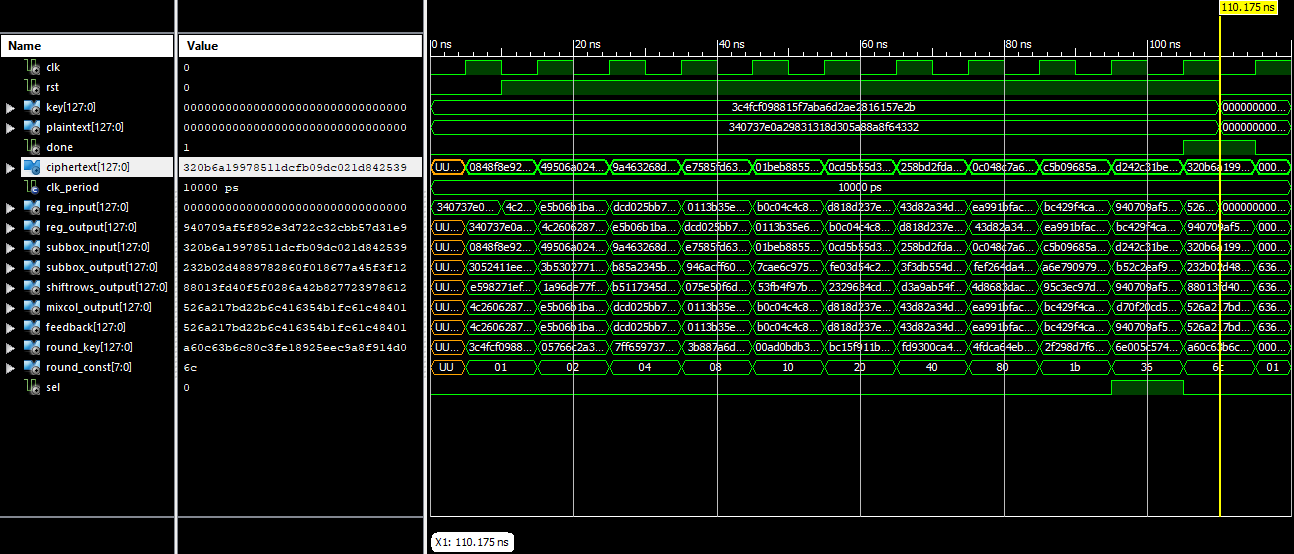
Test Vector
To validate the correctness of this implementation, I’ve used the test vectors provided by NIST, which is publicly avialble via the following link:
For example, according to the NIST reference, the encryption of plaintext 6BC1BEE2 2E409F96 E93D7E11 7393172A under the key 2B7E1516 28AED2A6 ABF71588 09CF4F3C, must yield the ciphertext: 3AD77BB4 0D7A3660 A89ECAF3 2466EF97. It should be noted that in these representations each byte is denoted by two hex digits. However, the bytes are arranged column-wise. Hence, to convert these representations into the 128-bit hex values, the order of bytes should be reversed as the last cell (bottom right) in the state array of AES has been considered the most significant byte in my implementation. For instance, the hex vectors corresponding to the above test vectors in our implementation are as follows:
plaintext:  x"2a179373117e3de9969f402ee2bec16b"
key:        x"3c4fcf098815f7aba6d2ae2816157e2b"
ciphertext: x"97ef6624f3ca9ea860367a0db47bd73a"
Decryption
In order to implement the decryption algorithm of AES-128, one must invert the SubBytes, ShiftRows and MixColumns operations. Let’s depict the inverse of SubBytes, ShiftRows and MixColumns operations by InvSubBytes, InvShiftRows and InvMixColumns respectively
While the area required to implement InvSubBytes and InvShiftRows are the same as the area required for implementation of SubBytes and ShiftRows respectively, the hardware implementation of InvMixColumns is a challenging problem since it’s matrix is more dense than the MixColumn’s matrix and therefore, uses more area than the MixColumns. In this implementation we use a technique taken from page 55 of [1] to overcome this problem. According to this technique, InvMixColumns can be implemented as a simple preprocessing step followed by the MixColumn step.
For a given key, the sub-keys must be used in reverse order to decrypt a ciphertext. Therefore, the encryption’s keyschedule can not be used for the decryption and a different keyschedule algorithm is needed. If one has access to the last round sub-key and perform the inverse of keyschedule round function on it repeatedly, sub-keys are obtained in reverse order. In our implementation for decryption algorithm, it is assumed that the last round sub-key is stored as the decryption key for the later reuse and it is assumed to be the input of the decryption’s keyschedule algorithm.
Architecture

Synthesis Report (Spartan6-xc6slx75-3fgg676)
You can find the details here: report
Advanced HDL Synthesis Report
=========================================================================
Macro Statistics
# RAMs                                                 : 20
 256x8-bit single-port distributed Read Only RAM       : 20
# Adders/Subtractors                                   : 2
 5-bit adder                                           : 1
 8-bit subtractor                                      : 1
# Registers                                            : 260
 Flip-Flops                                            : 260
# Multiplexers                                         : 3
 128-bit 2-to-1 multiplexer                            : 3
# Xors                                                 : 107
 128-bit xor2                                          : 1
 24-bit xor2                                           : 1
 32-bit xor2                                           : 3
 8-bit xor2                                            : 86
 8-bit xor3                                            : 16
=========================================================================
Device Utilization Summary
---------------------------

Selected Device : 6slx75fgg676-3

Slice Logic Utilization:
 Number of Slice Registers:             264  out of  93296     0%
 Number of Slice LUTs:                 1474  out of  46648     3%
    Number used as Logic:              1474  out of  46648     3%

Slice Logic Distribution:
 Number of LUT Flip Flop pairs used:   1478
   Number with an unused Flip Flop:    1214  out of   1478    82%
   Number with an unused LUT:             4  out of   1478     0%
   Number of fully used LUT-FF pairs:   260  out of   1478    17%
   Number of unique control sets:         2

IO Utilization:
 Number of IOs:                         387
 Number of bonded IOBs:                 387  out of    408    94%

Specific Feature Utilization:
 Number of BUFG/BUFGCTRLs:                1  out of     16     6%
Timing Summary
---------------
Speed Grade: -3

   Minimum period: 6.740ns (Maximum Frequency: 148.361MHz)
   Minimum input arrival time before clock: 4.726ns
   Maximum output required time after clock: 5.102ns
   Maximum combinational path delay: No path found
Throughput
According to the synthesis report produced by the ISE Design Suite, the minimum clock period for our implementation when Spartan6-xc6slx75-3fgg676 is used as the target device is 6.740 nano seconds. Therefore the throughput is equal to:
128 bits/(10*6.740 ns) = 1.90 Gb/s.
Synthesis Report (Artix7-xc7a200t-3-ffg1156)
You can find the details here: report
Advanced HDL Synthesis Report
=========================================================================
Macro Statistics
# RAMs                                                 : 20
 256x8-bit single-port distributed Read Only RAM       : 20
# Adders/Subtractors                                   : 2
 5-bit adder                                           : 1
 8-bit subtractor                                      : 1
# Registers                                            : 260
 Flip-Flops                                            : 260
# Multiplexers                                         : 3
 128-bit 2-to-1 multiplexer                            : 3
# Xors                                                 : 107
 128-bit xor2                                          : 1
 24-bit xor2                                           : 1
 32-bit xor2                                           : 3
 8-bit xor2                                            : 86
 8-bit xor3                                            : 16
=========================================================================
Device Utilization Summary
---------------------------
Selected Device : 7a200tffg1156-3

Slice Logic Utilization:
 Number of Slice Registers:             260  out of  269200     0%
 Number of Slice LUTs:                 1490  out of  134600     1%
    Number used as Logic:              1490  out of  134600     1%

Slice Logic Distribution:
 Number of LUT Flip Flop pairs used:   1490
   Number with an unused Flip Flop:    1230  out of   1490    82%
   Number with an unused LUT:             0  out of   1490     0%
   Number of fully used LUT-FF pairs:   260  out of   1490    17%
   Number of unique control sets:         2

IO Utilization:
 Number of IOs:                         387
 Number of bonded IOBs:                 387  out of    500    77%

Specific Feature Utilization:
 Number of BUFG/BUFGCTRLs:                1  out of     32     3%
Timing Summary
---------------
Speed Grade: -3

   Minimum period: 3.940ns (Maximum Frequency: 253.790MHz)
   Minimum input arrival time before clock: 1.177ns
   Maximum output required time after clock: 1.356ns
   Maximum combinational path delay: No path found
Throughput
According to the synthesis report produced by the ISE Designe Suite, the minimum clock period for our implementation when Artix7-xc7a200t-3-ffg1156 is used as the target device is 3.940 nano seconds. Therefore the throughput is equal to:
128 bits/(10*3.940 ns) = 3.25 Gb/s.
Synthesis Report (Zynq-xc7z100-2-ffg1156)
You can find the details here: report
Advanced HDL Synthesis Report
=========================================================================
Macro Statistics
# RAMs                                                 : 20
 256x8-bit single-port distributed Read Only RAM       : 20
# Adders/Subtractors                                   : 2
 5-bit adder                                           : 1
 8-bit subtractor                                      : 1
# Registers                                            : 260
 Flip-Flops                                            : 260
# Multiplexers                                         : 3
 128-bit 2-to-1 multiplexer                            : 3
# Xors                                                 : 107
 128-bit xor2                                          : 1
 24-bit xor2                                           : 1
 32-bit xor2                                           : 3
 8-bit xor2                                            : 86
 8-bit xor3                                            : 16
=========================================================================
Device Utilization Summary
---------------------------
Selected Device : 7z100ffg1156-2

Slice Logic Utilization:
 Number of Slice Registers:             260  out of  554800     0%
 Number of Slice LUTs:                 1490  out of  277400     0%
    Number used as Logic:              1490  out of  277400     0%

Slice Logic Distribution:
 Number of LUT Flip Flop pairs used:   1490
   Number with an unused Flip Flop:    1230  out of   1490    82%
   Number with an unused LUT:             0  out of   1490     0%
   Number of fully used LUT-FF pairs:   260  out of   1490    17%
   Number of unique control sets:         2

IO Utilization:
 Number of IOs:                         387
 Number of bonded IOBs:                 387  out of    400    96%

Specific Feature Utilization:
 Number of BUFG/BUFGCTRLs:                1  out of     32     3%
Timing Summary
---------------
Speed Grade: -2

   Minimum period: 3.324ns (Maximum Frequency: 300.806MHz)
   Minimum input arrival time before clock: 1.185ns
   Maximum output required time after clock: 1.243ns
   Maximum combinational path delay: No path found
Throughput
According to the synthesis report produced by the ISE Designe Suite, the minimum clock period for our implementation when Zynq-xc7z100-2-ffg1156 is used as the target device is 3.324 nano seconds. Therefore the throughput is equal to:
128 bits/(10*3.324 ns) = 3.85 Gb/s.
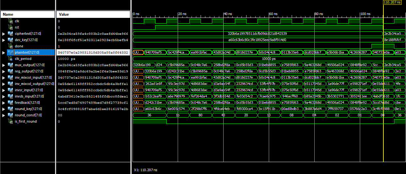
Simulation
In order to verify the correctness of the decryption’s implementation, a testbech has been prepared in which the equality of the derived plaintext with the refernce values taken from [1] is checked for two different ciphertexts and keys. As you can see in the following picture, this implementation passes the verification and hence it works correctly.
References
[1] The Design of Rijndael: AES - The Advanced Encryption Standard